| Category |
Coursework |
Subject |
Engineering |
| University |
|
Module Title |
Related to Semiconductor Fundamentals |
Fabrication and Testing of Schottky Diodes- Lab1
I. Learning:
a) Familiarize students with the operation of advance fabrication and testing facilities used in semiconductor industries (such as, deposition of high purity metals, vacuum evaporator, diffusion furnace, clean room, probe station, electrical-meters, etc.)
b) Probing semiconductor devices and measurement of their electrical characteristics.
c) Data analysis and interpretation (Electrical and statistical).
d) Applications of Schottky diode (through independent study by the students).
II. Introduction
A Schottky diode is a metal-semiconductor rectifying junction, Figure 1 shows a crosssection view of Schottky diode.

The Schottky diode is a “majority carrier” semiconductor device, with reference to Figure- 1, where the body can be n or p -type (in your case, it will be p-type), then the majority carriers, depending on the type of the substrate, either electrons or holes. The electrons
or holes are quickly injected into the conduction band of the metal contact, to become free moving electrons or holes, thus not having the random recombination of electrons and holes as in a normal PN junction diode, which gives a faster switching time.
Ohmic contact: - This kind of electrical contact has low resistance and symmetric current flow in both directions (reverse and forward bias), hence this contact is also called as non- rectifying contact (as shown in the following voltage (V) vs current density (J) behaviour.

Non-ohmic contact: This type of electrical contact has an asymmetric current flow when compared to negative and positive voltage directions (reverse and forward bias). This type of contact is referred to as a rectifying contact or Schottky (as shown in the behaviour of voltage (V) vs current density (J)).

Metal in contact with the semiconductor (p-type or n-type) results in bending of bands; which is a consequence of charges that actually flow across the interface of metal and semiconductor. These two types of contacts are well understood with the aid of energy band diagrams. Prior to band diagrams one has to understand concepts of work function. The minimum energy required to take out an electron from the Fermi level to vacuum level for metal and/or semiconductor is called as the work function of metal (ɸm) and electronegativity of semiconductor (ɸs) respectively. When a metal and semiconductor which have different (not same value) work function and electronegativity are brought into contact, Fermi levels are forced to align and energy band diagrams for such configuration are shown in Figure 2.

Figure 2. Band diagram of Schottky contact (a) and ohmic contact (b) between a metal and p-type semiconductor, showing Fermi energy (EF), intrinsic band (EI), valance band (EV) and conduction band (EC).
For simpler understanding, let us consider empty states in metal which exponentially decrease with energy below the Fermi level for holes. For ɸm < ɸs contact; at equilibrium there is a barrier to the flow of holes in both directions. If EFM (Fermi level of metal) is moved upwards corresponding to EFS (Fermi level semiconductor), a barrier is reduced so that holes flow from semiconductor to metal. This results in hole current from semiconductor to metal which increases exponentially with increased separation between EFM and EFS. When bias is reversed, flow of holes from semiconductor to metal is blocked and slow saturation of hole current is observed which is actually from metal to semiconductor. Hence, when ɸm < ɸs, established contact is rectifying which in other words called as non-ohmic contact and shows asymmetric J-V characteristics.
Ohmic contact can be obtained if we somehow manage to bend semiconductor band upwards. When a band bends upwards; edge of valence band will get closer to Fermi level or sometimes cross Fermi level. Now let us consider ɸm > ɸs contact; at equilibrium there is no barrier for flow of holes from semiconductor to metal. However, a small barrier for flow of holes from metal to semiconductor can be removed if EFM is moved slightly lower corresponding to EFS. Hence, when ɸm > ɸs, established contact is non- rectifying, which in other words called as ohmic contact and shows symmetrical J-V characteristics as.
Relationship between junction capacitance and applied voltage
The junction capacitance is dependent on the width of the depletion layer, however, this is not constant as it varies with the applied voltage across it, and hence the value of capacitance varies.
The depletion layer capacitance per unit area is defined as:
𝐶𝐷
= 𝑑𝑄𝐷
𝑑𝑉
Equation 1
Which is a change in charge for a change in applied voltage.
The depletion layer capacitance CD (capacitance/area) can be calculated from the equation for a parallel plate capacitor, which is: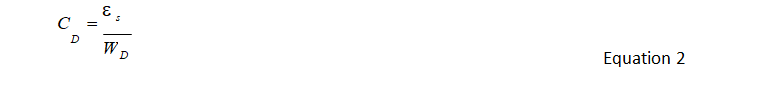

Where;

Where;


The information that can be obtained from the graph, by interpolation the built-in potential bi , this is where 1/C 2 = 0, and the dopingDdensity N (or acceptor density; if the substrate is p-type doped).
Relationship between Current-Voltage The current-voltage behaviour of Schottky diodes is given by the following relationship

Where, I is the current, Is is the saturation current, e is the electronic charge, V is the applied voltage, k is Boltzmann’s constant, T is the absolute temperature and (Greek letter eta) is a constant in the range 1 to 2 for commercial available diodes.
References
1. Febin Paul, Krishna Nama Manjunatha, Sridhar Govindarajan, Shashi Paul, Single step ohmic contact for heavily doped n-type silicon, Applied Surface Science, Volume 506, 2020, 144686, j.apsusc
2. Physics of Semiconductor Devices by S.M Sze.
 Get Expert-crafted assignments