Looking for Plagiarism-Free Answers for Your US, UK, Singapore, New Zealand, and Ireland College/University Assignments?
Talk to an Expert| Category | Assignment | Subject | Engineering |
|---|---|---|---|
| University | Uxbridge College (UC) | Module Title | Unit 4019 Electrical and Electronic Principles |
In Physical lab 2, Activity II – “Find the internal resistance of the battery”, you tried to find the internal resistance (R1) of a 1.5V battery.
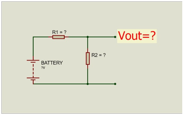
Figure 1. Schematic circuit to find internal resistance, physical lab 2.
Your lecturer MUST confirm that you did this in the lab.
Referring to Figure 1,
Show the pictures of your assembled circuit on breadboard.
Show your measured value for the battery voltage (Vbattery) and R2.
Explain the operation of that circuit. In particular,
– Using Ohm’s law and voltage division, calculate R1.
– Show your calculation for R1.
Measured Values:
Battery voltage: Vbattery = 3,307 V
Resistor: R2 = 986Ω
Output voltage: Vout = 3,284V
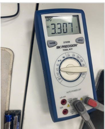
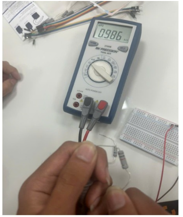
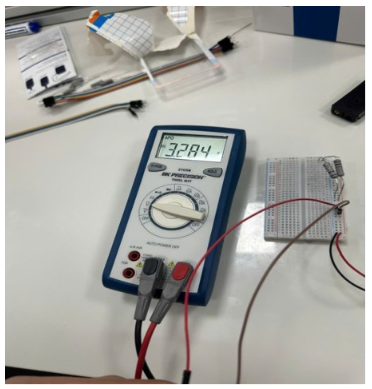
Circuit structure analysis: The circuit is a simple voltage divider. The internal resistance R1 can be calculated.
1.1) Find R1:
Apply Voltage Division rule:
Formula: Vout = Vbattery × R_2/(R_2+R_1 )
Vout/Vbattery= R_2/(R_2+R_1 ) => R1 = R2(V_battery/Vout-1) R1 = 986(3,307/3,284-1) ≈ 6,9056Ω
In Physical lab 2, Activity III – “Resistor in series and in parallel”, you experimented a circuit with resistors in series and in parallel. Applying several laws of circuit theory, you will now explain the operation of this circuit, by answering the following questions:
a) Series resistors (Figure 2)
Figure 2. Schematic circuit of resistors in series, physical lab 2.
Your lecturer MUST confirmed that you did this in the lab.
Referring to Figure 2,
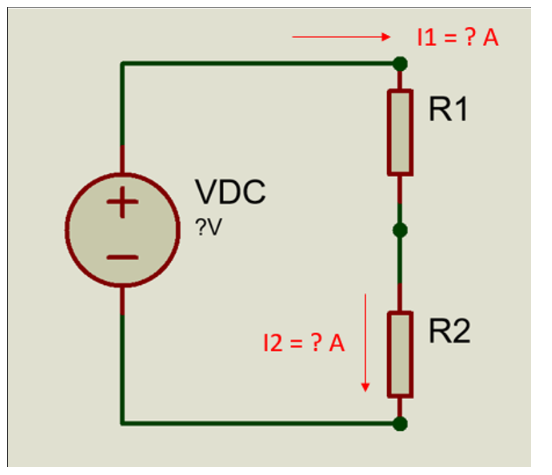
i) Show pictures of your assembled circuit on breadboard.
ii) Show your measured value for I1, I2, R1, R2 and VDC.
iii) Using Ohm’s law, calculate V1 = I1 × R1 and V2 = I2 × R2. Are your results the same as the measured values V1 and V2?
Measured Values:
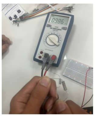
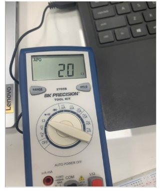
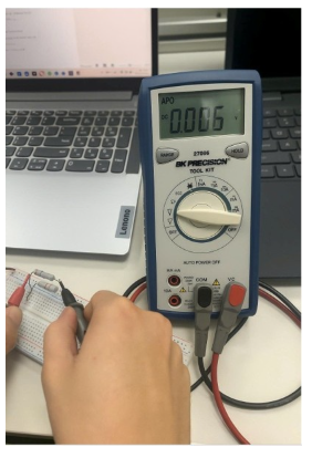
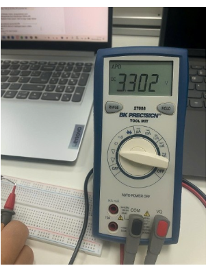
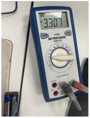
Total resistance: R = R1 + R2 = 2 + 986 = 988Ω
Total voltage: VDC = V1 + V2 = 0,003 + 3,305 = 3,308V
Current of circuit: I = VDC/R = 3,308/988 ≈ 0,00335A
Check again with Ohm’s Law:
V1 = I × R1 = 0,00355 × 2 ≈ 0,006V
V2 = I × R2 = 0,00355 × 988 ≈ 3,302V
I1 = V1/R1 = 0,006/2 = 0,003A
I2 = V2/R2 = 3,302/986 ≈ 0,00335A
b) Parallel resistors (Figure 3)
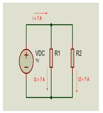
Figure 3. Schematic circuit of resistors in parallel, physical lab 2.
Your lecturer MUST confirmed that you did this in the lab.
Referring to Figure 3,
i) Show pictures of your assembled circuit on breadboard.
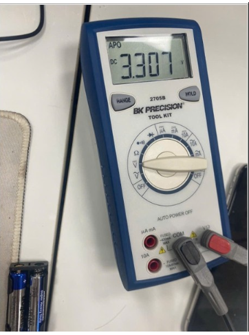
ii) Show your measured value for I1, I2, R1, R2 and VDC.
iii) Is I = I1 + I2? Show your calculation. What law is this?
iv) Is /1 = R2/R1+R2*I ? Show your calculation. What law is this?
Battery voltage: VDC = Vbattery = 3,307 V
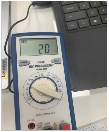
Resistor: R1 = 2Ω
Resistor: R2 = 986Ω
Calculated values included in document:
Total resistance: R = R1R2/(R1+R2)= (2×986)/(2+986)= 493/247Ω
Apply Ohm’s Law: I = V/R = (3,307)/(493/247) ≈ 1,656853A
Check if I = I1 + I2
VDC = V1 = V2 = 3,307V( 2 parallel resistors)
I1 = V1/R1= (3,307)/2= 1,6535A
I2 = V2/R2= (3,307)/986 ≈ 0,003353A
Total Current I = I1 + I2 = 1,6535 + 0,003353 = 1,656853A
So the summary is correct
Check if I1= R2/(R1+R2)×I
I1 = V1/R1= (3,307)/2= 1,6535A
R2/(R1+R2)×I = R2/(R1+R2) × V/R= (2×986)/(2+986) × (3,307)/(493/247) = 1,6535A
So the equation is correct
Explain the operation of the circuit in Figure 4:
Apply Ohm’s law, Kirchhoff’s laws and Mesh or Nodal analysis
Find V0 and the power over the 3𝝮 resistor in the circuit of Figure 4
Show your calculation
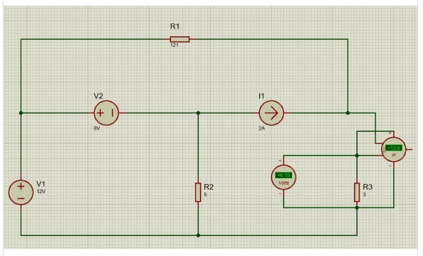
Use Proteus to check your result. Add pictures of your simulated circuit and simulated result.
n is a random number given by the lecturer for each student.
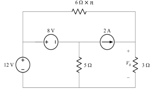
Figure 4
Give n number: 21
v_1=12V,v_2=v_1-8=4V
I=I_1+I_2
I_2=2+I_3
=>I=I_1+I_3+2(1)
Apply Ohm’s Law and given data
=>I_1=(v_1-v_0)/R=(12-v_0)/126 (2)
I_3=v_2/5=4/5
v_0=(3I_1+2)(3)
Replace (3) with (2)
v_0=3((12-v_0)/126+2)
=>v_0=264/43 V
P=v^2/R=(264/43)^2/3≈12,6W
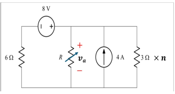
In the circuit shown in Figure 5, where n is a random number given by lecturer for each student, R is a Variable resistor.
Examine the circuit, then answer the following questions about its operation:
In case R = 6𝝮,
Use superposition to obtain va in the circuit of Figure 5.
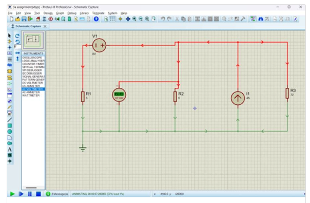
Show your work and use Proteus to check the value of va.
Add pictures of your simulated circuit and simulated result.
Circuit has:
Voltage source 8V
Current source 4A
R1 = 6(Variable resistor), R2 = 3.21 = 63(n=21)
Considering 8V (turn off 4A – replacing with a short circuit)
1/R_z =1/R_1 +1/R_2 =1/6+1/63=23/126⇒R_z=126/23 Ω
R_t=R_z+R_1=126/23+6=264/23 Ω
Apply Ohm’s law:
I=V/Rt=8/(264/23)=23/33 A
V_(a_1 )=R_z×I=126/23×23/33=42/11 V
Considering 4A (turn off 8V – replacing with a short circuit)
V_(a_2 )/6+V_(a_2 )/6+V_(a_2 )/63=4⇒V_(a_2 )=126/11 V
Using the superposition theorem, the total voltage is:
V_a=V_(a_1 )+V_(a_2 )=42/11+126/11=15,27V
b.Compute the value of R that results in maximum power transfer in the circuit of Figure 5.
Find the maximum power.
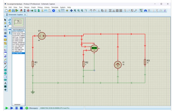
Show your work and use Proteus to check your answer.
Add pictures of your simulated circuit and simulated result.
Using Thevenin’s Theorem
Replace the 8V voltage source Short circuit (wire)
Replace the 4A voltage source Open circuit
Thevenin resistance:
R_th=(6×63)/(6+63)=126/23 Ω
Thevenin voltage:
(v-v_th)/R_1 +I=v_th/R_2 ⇒(8-v_th)/6+4=v_th/63⇒v_th≈29.21739V
Maximum power transfer in the circuit:
P_(m=(v_th )^2/(4R_th ))=〖29,22〗^2/(4.126/23)=38,96W
Analyse the RLC circuit below (Figure 6) and:
Find the steady-state voltage over the inductor and the current going through the inductor.
Show your work.
Each student receives a different ω value (rad/s) from the lecturer.
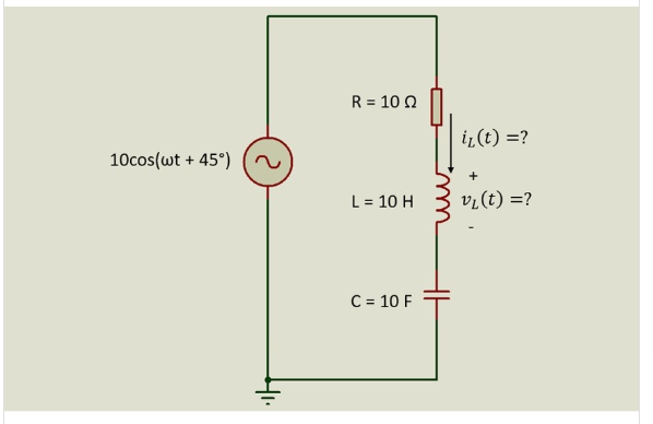
Circuit has:
R = z_R = 10Ω
L = 10H
C = 10F
V(t) = 10cos(ωt + 45^0) = V_S = 10∠45° (V)
ω = 21(rad/s)
Impedance of inductor: z_L= jωL =j .21.10 = j210Ω
Impedance of capacitor: z_C=1/jωC= 1/(j⋅21.10)=-1/j210≈ -j0.004761904761904762Ω
Equivalent impedance: z_eq=z_R+z_L+z_C= 10 + j210 – j0.004761904761904762Ω
= 10 + j209.9952380952381(Ω)
Find i_L (t):
Modulus:|Z|= √(Z^2+X^2 )= √(10^2+(209,9952)^2 ) = 210,233Ω
Phase angle of the sum:∅=〖tan〗^(-1) (X/R)= 〖tan〗^(-1) (209,9952/10)≈87,27°
i_L (t)= V_S/z_eq = (10∠45°)/(210.233∠87,27°) ≈ 0,047566∠-42,27°
Find v_L (t):
v_L (t) = I.Z = 0,047566∠-42,27°.240 = 9.98886∠47,73°
In Figure 7 below, analyse the combined RLC circuit and determine the phasor voltage V.
Show your work.
In the process:
Use Kirchhoff’s laws, Ohm’s law and Mesh or Nodal analysis for AC circuit
Transform between complex number and phasor
Each student receives a different n value from the lecturer
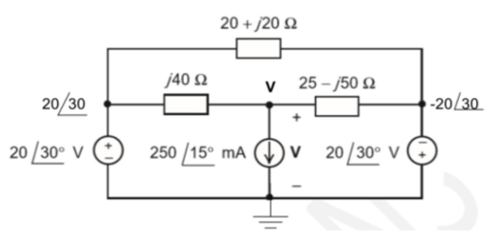
Given
n = 21
V_L = 20∠30°
V_R = 20∠-30°
I = 250∠15° mA = 0,25∠15°A
Z_1 = 20 + j20 (Ω)
Z_2= n.j40 = 21.j40 = j840 (Ω)
Z_3 = 25 – j50 (Ω)
Apply KCL at node V:
Current through: Z_1: I_1 = (V-(20∠〖30〗^0 ))/Z_1 =(V-(20∠〖30〗^0 ))/(20+j20)
Z_2: I_2 = v/Z_2 = V/j840
Z_3: I_3 = (V-(20∠〖30〗^0 ))/Z_1 = (V-(20∠-〖30〗^0 ))/(25+j50)
Total equation at node V: I_1 + I_2 + I_3 – I = 0
(V-(20∠〖30〗^0 ))/(20+j20) + V/j840 + (V-(20∠-〖30〗^0 ))/(25+j50) – 0,25∠15° = 0
V((1-(20∠30^0 ))/(20+j20) + 1/j840 + (1- (20∠-30^0 ))/(25+j50)) – 0,25∠15° = 0
V(1/(20+j20) + 1/j840 + 1/(25+j50)) = ((20∠30^0 ))/(20+j20) + ((20∠-30^0 ))/(25+j50) + 0,25∠15°
Compute the complex quatities:
1/(20+j20)= (20- j20)/((20+j20)(20-j20))=(20- j20)/800= 0,025 – j0,025
1/j840 ≈ -j1.190476.10^(-3)
1/(25+j50) = (25- j50)/((25+j50)(25-j50)) = (25- j50)/3125 = 8. 〖10〗^(-3)+ 16. 〖10〗^(-3)
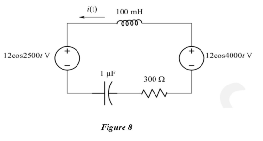
Evaluate the operation and behaviour of the series RLC circuit in Figure 8 by doing the following steps:
Each student receives a different value of n from the lecturer.
Answer the following questions:
a) Describe the voltage condition for a PN junction to conduct current. Draw or add picture for the I-V graph of a diode.
b) Describe the voltage condition for an NPN transistor to conduct current. Illustrate your answer using the NPN transistor symbol.
c) Describe the voltage condition for a PNP transistor to conduct current. Illustrate your answer using the PNP transistor symbol.
Problem 2:
In Physical lab 5, you already demonstrated the action of diodes by implementing a full-wave rectifier, both in practical and analytical settings.
a) Show pictures of your assembled circuits on breadboard, and the relevant oscilloscope measurements in Physical lab 5.
Your lecturer MUST confirm that you did the lab.
b) Based on your assembled circuits in Physical lab 5, explain shortly:
– Which property of the diodes allow us to convert an AC signal to DC signal?
– How did capacitors help smoothing out the circuit?
Explain the main difference between digital and analogue electronics. Draw or add pictures for analogue and digital signals.
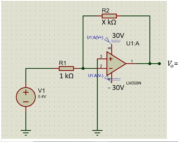
Explain the operation of the inverting amplifier in Figure 1 in analytical setting:
For practical setting, use Proteus to check your result. Add pictures of your simulated circuit and simulated result.
Figure 1. Inverting amplifier
The application of “Binary Decoder” to control the lamp system is described in Figure 2. The “Binary Decoder” using Logic gates is described in Figure 3.
Figure 2. Lamp controlling system
Figure 3. Logic circuit of the binary decoder
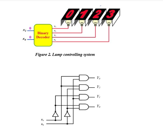
Examine the circuit above:
Draw the truth table for each output.
Assuming that the lamps are Active-High, determine the status of the lamps (on or off) when X0 = 1 (High) and X1 =0 (Low).
a) Analyse the operation of a PN junction. Your answer must include the concepts of doping, holes, electrons, depletion region, forward bias, and reverse bias.
b) Analyse the operation of a bipolar NPN transistor. Your answer must include the concepts of doping, depletion region, forward bias, and reverse bias.
c) Analyse the operation of a bipolar PNP transistor. Your answer must include the concepts of doping, depletion region, forward bias, and reverse bias.
Critique the benefits and drawbacks of using analogue and digital electronic devices using examples.
a) When will a diode break down? Explain using the concept of reverse bias, depletion region and current direction.
b) Zener diode is widely used for its breakdown property. Discuss why we DID NOT use a Zener diode in Physical Lab 5. Use simple semiconductor theory in your answer.
c) Discuss why we can use BJT transistors to amplify signals. Use simple semiconductor theory in your answer.
Reflecting on your experience in Physical Lab 5,
a) Evaluate the role of analogue electronic circuits in supplying power to a device.
b) Evaluate the role of digital electronic circuits in supplying power to a device.
Need plagiarism-free Answers for your college/ university Assignments
Order Non-Plagiarised AssignmentAre you facing problems with your BTEC Level 5 Unit 4019 Electrical & Electronic Principles Assignment Report? Get expert assignment help in UK from top-rated professionals! Whether you're thinking, "Can someone do my assignment for me?" or looking to boost your grades with quality reference material, we've got you covered. Access a free list of assignment samples written by professional PhD writers and see how top-tier academic support can transform your studies. Don’t settle for less—get the help you deserve today!
Hire Assignment Helper Today!
Let's Book Your Work with Our Expert and Get High-Quality Content
