Looking for Plagiarism-Free Answers for Your US, UK, Singapore, New Zealand, and Ireland College/University Assignments?
Talk to an Expert| Category | Assignment | Subject | Engineering |
|---|---|---|---|
| University | The University of New South Wales (UNSW Sydney) | Module Title | ELEC2133 Analogue Electronics |
| Assessment Type | Assignment 1 |
|---|---|
| Academic Year | 2025 |
| Due Date: | Thursday, July 17, 2025, by 9:00 AM |
The assignment consists of two problems, each containing four parts. Each part includes one or more questions related to topics on operational amplifiers (op-amps)and transistor amplifiers.
Each question is labelled with one of the following difficulty levels:
P (Pass):Correctly answering these questions demonstrates a pass-level understanding.
C (Credit):Correctly answering these questions demonstrates a credit-level performance.
D (Distinction):Designed for students targeting a distinction.
HD (High Distinction):For students aiming for the highest level of achievement.
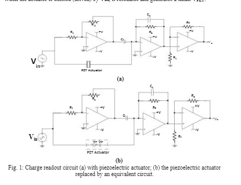
The circuit shown in Fig. 1(a) is a sensor readout circuit developed by the MEMS/NEMS research group at EE&T, UNSW. Though simple in design, it is highly effective for amplifying the small electrical signal (voltage) generated by a PZT thin film in a micro-lens actuator during resonance.
PZT, or lead zirconate titanate, is a piezoelectric material that converts mechanical strain into electrical charge (voltage), and vice versa—applied voltage into mechanical strain. This dual functionality makes PZT ideal for constructing actuators, which are devices that convert electrical energy into mechanical motion. Piezoelectric actuators enable extremely precise nanoscale movements and are widely used in advanced instrumentation, robotics, automotive systems, energy harvesting devices, and more.
In addition to actuators, PZT is also used in sensors to detect minute movements, pressure, and forces. Applications include touch screens, pressure sensors, accelerometers, gyroscopes, and other precision sensing technologies.
Fig. 1(b) shows the sensor readout circuit with the PZTactuator replaced by its electrical equivalent circuit that consists of a voltage source (VPZT) in series with a capacitor (CPZT ). When the actuator is excited (driven) by Vin, it resonates and generates a small VPZT .

Do You Need ELEC2133 Assignment 1 of This Question
Order Non Plagiarized AssignmentIn reference to Fig. 1(a), the op-amps have large signal limitations and other characteristics as provided in Table 1. Assuming the bandwidth of the readout circuit is limited by the non- inverting amplifier stage (the last stage) and R = 1k and R3 = 280k
(a) [P, C] Estimate the bandwidth of the readout circuit.
(b) [P, C] With Vin = VACOS(cot) and V1V and assuming VPZT = 0.005 Vin, will there be a frequency at which the output (V.) will be distorted? If so, what is that frequency?
(c) [D] With Vin = Vacos(2*900t) and assuming Rs = 0.5M2, R4 = 1km, R3 = 280kn, R1 lkn R1=lkn, C1 = C2 = CPZT = 10nf, what is the constrain on the Va if the output is to be undistorted?
(a) [HD] In the non-ideal case, the non-inverting op-amp (last stage) in Fig. 1 has the following DC imperfections. Assume all the other op-amps are ideal.
Input bias current: Is 40nA at room temperature Input offset current: Iio = ±2nA at room temperature Input offset voltage: Vio=2mV at room temperature Calculate the worst-case output offset voltage at room temperature assuming Rs 500kn, R4=1k, R1 = 280kn, R1=lkn, R=1kn, C1 = C2 = CPZT = 10nf. [Hint: Consider the DC imperfections in all the op-amps. In DC, capacitor can be regarded as open]
[P.C] Using LTspice or Pspice simulation, confirm your answer for part 1(c), part 2(a), part 3 (a). You may use LM301 op-amp and its model for the simulation. The op-amp is used in the first lab.
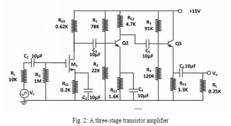
In Question 1, you analysed and designed the charge readout circuit for the PZT actuator shown in Fig. 1(a). A common issue with this circuit is that the final stage—the non-inverting amplifier—tends to amplify low-frequency noise originating from the power supply or environmental vibrations affecting the actuator. Additionally, it can amplify any DC offsets introduced by earlier stages in the circuit. Minimizing output noise while maintaining adequate signal amplification is crucial. Although there are various ways to improve the signal-to-noise ratio of the non-inverting amplifier, in this assignment it will be replaced with a three-stage transistor amplifier, as shown in Fig. 2(a). Your task is to analyse this new amplifier by calculating its gain, input and output impedance, and bandwidth.

The three-stage amplifier consists of one n-channel MOSFET transistor Q1 in depletion mode with W/L = 1 and two BJT transistors Q1and Q2 . The transistors have the model parameters as provided in the table below.

(a)[P] Identify the amplifier configuration used in each stage of the amplifier.[1.5 marks]
(b)[P,C] what are the functions of C1, C2, C3, C4, and C5 capacitors? [1.5 marks] (c)[P,C] Explain what are the purposes of each amplifier, and can a single-stage transistor amplifier (say stage 1 or 2 or 3) be used instead?
(a) [P] Draw the DC equivalent circuit of the transistor amplifier in Fig. 2. Note that capacitors act as open circuit in DC conditions.
(b) [P.C]Show that the Q-Point values are: M1(1=5mA, V1s=10.9V), Q1 (L=1.51mA, VCE = 5.49V), and Q2 (1.99mA, 8.44V).
(c) [P.C] Calculate the transistor model parameters for each transistor, namely gml, gm2, gm3, 161, 102, 13, 1-2 and r [2 marks]
(d) [D] *Comment on the possible range of resistance values that may replace the Rc2 = 4.7km, Ro2 = 0.62k of the BJT Q1 transistor in the amplifier. [Hint: BJT must operate in a forward-active region and MOSFET must operate in a saturation region] [3 marks]
(a) [P,C] Draw small-signal equivalent circuit of the amplifier in the form suitable for low frequency.
(b) [D] Calculate the lower 3dB frequency, £, of the amplifier using the appropriate time constant method. [4.5 marks]
(c) [P.C] Draw small-signal equivalent circuit of the amplifier in the form suitable for high-frequency analysis.
(d) [DN, HD] Calculate the higher 3dB frequency, f, of the amplifier using the appropriate time constant method.
(a) [DN] Simulate Fig. 2 and compare the results with your calculation of midband gain and bandwidth. The Spice transistor models will be uploaded on Moodle.
Achieve Higher Grades ELEC2133 Assignment 1
Order Non Plagiarized AssignmentLooking for expert guidance in ELEC2133 Analogue Electronics Assignment 1? Worry, no need! We are here to help you with assignments. Whether you need Electrical Engineering Assignment Help or well-structured solutions, we will provide everything. You will get free assignment examples that will make your study material stronger. Our expert team is providing all assignment services, you will get accurate, clear, and original content. Now stop worrying about marks and complete your assignments hassle-free with expert support. So what's the delay? Get connected with us now and make your academic journey easy!
Hire Assignment Helper Today!
Let's Book Your Work with Our Expert and Get High-Quality Content
